E3S REU Participants and Projects: 2017
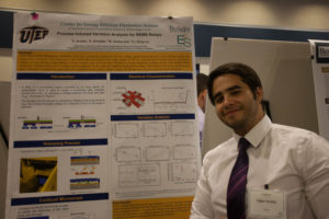
Undergraduate Researcher: Edgar Acosta
Major: Electrical Engineering
Home Institution: University of Texas, El Paso
Research Project:Process Induced Variation Analysis for NEMS Relays
Faculty Advisor: Prof. Tsu-Jae King Liu
Graduate Student Mentor: Sergio Almeida
Hosting Organization: Department of Electrical Engineering and Computer Sciences, University of California, Berkeley
Project Abstract: Nano/Microelectro-Mechanical (N/MEM) relays are a promising prospective for low voltage digital electronics due to zero leakage current and steep off/on transition. It has been shown that NEM relays can operate with a gate voltage of 100 mV with the help of a body bias [1]. The pull in voltage of such devices is the addition of both voltages, gate and body bias. Therefore, to make functional complex circuits with multiple NEM relays the variation of the pull in voltage must be analysed. In this work, the variation of the pull in voltage with respect to the device thickness and gap is analysed. It is found the gap is the main contributor to the pull in voltage change, but this gap also correlates with the device thickness.
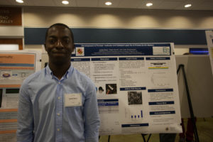
Undergraduate Researcher: Joubel Boco
Major: Electrical Engineering
Home Institution: University of Maryland – College Park
Research Project:Development of Printed Cathode and Catalyst Layer for A Printed Zn-Air Battery
Faculty Advisor: Prof. Vivek Subramanian
Graduate Student Mentor: Rajan Kumar
Hosting Organization: Department of Materials Science and Engineering and Department of Electrical Engineering and Computer Science, University of California, Berkeley
Project Abstract: Printed electronics are currently limited by the development of printed energy storage. Zinc-air is a suitable battery chemistry for Internet of things (IoT) applications due to its high theoretical energy density, large storage capacity, and use of low cost, earth abundant materials. In order to design a printed Zn-air battery, several challenges must be addressed, including the slow oxygen reduction reaction that limits performance at high current. Thus, we aim to design an optimized cathode and a catalyst for a printed zinc-air battery. For this study, a carbon cathode and platinum catalyst were chosen, and factors such as cathode thickness and annealing conditions were explored. Several batches of printed zinc-air batteries were developed and their discharge performance was analyzed. Scanning electron microscopy (SEM) and energy dispersive X-ray spectroscopy (EDS) were also used to determine the optimal electrode structure. Finally, we developed a strategy for the top current collector and encapsulation layer for a packed full cell.
Undergraduate Researcher: Ryan Brandt

Major: Physics and Electrical Engineering
Home Institution: North Carolina State University
Research Project:Impact of Joule Heating on Potential Usage of LEDs for Solid-State Refrigeration
Faculty Advisor: Prof. Eli Yablonovitch
Graduate Student Mentor: Patrick Xiao
Hosting Organization: Department of Electrical Engineering and Computer Sciences, University of California, Berkeley
Project Abstract: LEDs convert electrons into photons, carrying entropy and energy away in the form of light. In each conversion, the energy of the emitted photon is equal to the band gap energy of the LED, and the energy lost by the electron is equal to qV, where V is the voltage across the LED and q is the fundamental charge. As it turns out, these energies are not the same, and indeed, energy must be absorbed from the LED in the form of heat to account for this difference at low voltage. This means that for an LED with high enough efficiency and minimal internal heating, a net cooling should be observed, allowing for LEDs to function as solid-state refrigerators. In order to design an LED capable of producing this cooling effect, it is desirable to create an accurate model of the system in order to better understand the electrical and thermodynamic properties of an LED. Using this model, the impact of particular design choices for an LED can be thoroughly analyzed, and hopefully lead to the development of an optimal design. An LED is a device with continuous distributions of voltages and currents inside it, which can be modeled as a network of infinitesimal nodes separated by resistors, diodes, and current courses. Using this model, a differential equation can be derived and solved for a particular LED design, allowing us to evaluate and optimize the LED design choices.
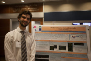
Undergraduate Researcher: David Friedman
Major: Physics
Home Institution: University of Illinois Urbana Champaign
Research Project: Photonic Layout Versus Schematic
Faculty Advisor: Somayeh Moazzeni
Hosting Organization: BWRC, Department of Electrical Engineering and Computer Science, University of California, Berkeley
Project Abstract: Silicon photonics is a promising technology that combines the standard electronic semiconductor platforms with micro scale optical devices to leverage the capabilities of existing microelectronics. One of the major applications of such devices is communication via photon emission over long distances; the advantages of these systems is that they can do so with minimal power dissipation, and with more data rate capacity than copper wires (Thomson). Although several such systems have been developed, their use is limited to a handful of optical and electrical devices due to lack of an adequate design flow large scale designs. Here, in ISG group, a photonic very large system integration (VLSI) flow has been developed to address this issue; additionally, the group has demonstrated such an optoelectronic system with millions of transistors and hundreds of photonic devices on a single die. The goal of the project this summer is to complete an important part of this flow known as photonic layout versus design (PLVS) verification, which is based on the existing LVS flow used in the pure electrical chip design process. This tool enables verification that the final chip design matches the initial chip schematic. The first step is to add photonic device recognition to the layout and run PLVS checks for a sample optical system.
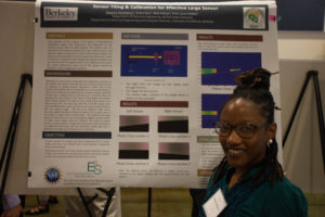
Undergraduate Researcher: Essence Hansberry
Major: Electrical Engineering
Home Institution: Norfolk State University
Research Project: Sensor Tiling & Calibration for Effective Large Sensor
Faculty Advisor: , Prof. Laura Waller
Graduate Student Mentor: Grace Kuo
Hosting Organization: Department of Electrical Engineering and Computer Science, University of California, Berkeley
Project Abstract: The purpose of this project is to create a computational calibration system that determines the alignment of two camera sensors that are tiled together. The system’s job is to determine the distance between the two camera sensors and also the angle at which one or both of them may be tilted. The sensors could possibly be microns away from each other, which is why this is important. After finding the distance between the two sensors and the angle at which one is tilted from the other, the system determines how one of the sensors should be shifted in order to align them properly.
Undergraduate Researcher: Emily Iwanski
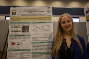
Major: Mechanical Engineering
Home Institution: University of Michigan
Research Project: Characterization of the Mechanical Time Delay in NEM Relays
Faculty Advisors: Prof. Tsu-Jae King Liu
Graduate Student Mentor: Urmita Sikder
Hosting Organization: Department of Electrical Engineering and Computer Sciences, University of California, Berkeley
Project Abstract: Nanoelectromechanical (NEM) relays provide an attractive option for ultra-low power digital logic since body biased operation potentially enables sub 100 mV switching. The mechanical time delay was measured, varying gate overdrive voltage and body bias, hence the effect of body bias on mechanical time delay was determined. Comparisons were made between the experimental data and a numerical model to gain insights into the dynamic performance of these relays. This study will allow for better optimization of NEM devices and the creation of a more accurate time delay model.
Undergraduate Researcher: Anudeep Mangu
Major: Engineering Physics
Home Institution: University of Illinois at Urbana-Champaign
Research Project: Optical Pumping of High Contrast Grating Vertical Cavity Surface Emitting Laser Test Structures
Faculty Advisor: Prof. Constance Chang-Hasnain
Graduate Student Mentor: Jonas Kapraun
Hosting Organization: Department of Electrical Engineering and Computer Science, University of California, Berkeley
Project Abstract: Electrically pumped, wavelength tunable vertical cavity surface emitting lasers (VCSELs) are good candidates for light sources in applications requiring a small size, low cost, and large tuning range. Full fabrication of electrically VCSEL devices requires 2 weeks of effort, preventing rapid design testing. This project aims to use optical pumping and photoluminescence spectroscopy to observe lasing behavior in test structures without electrical contacts in order to develop a new rapid testing technique for VCSELs.
Undergraduate Researcher: Matthew Rollings
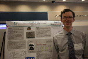
Major: Chemistry Home Institution: University of Massachusetts, Amherst
Research Project: Self-Assembled Monolayer to Improve MEM Switch Performance
Faculty Advisor: Prof. Tsu-Jae King Liu
Graduate Student Mentor: Jatlin Patin
Hosting Organization: Department of Electrical Engineering and Computer Science, University of California, Berkeley
Project Abstract: More sophisticated electronics require increasingly more power. Nanoscale electro-mechanical (NEM) relays offer zero OFF-state leakage current, allowing energy efficiency. However, they suffer from high actuation voltages, as well as ‘stuck-ON’ failure when adhesive forces, known as stiction, become insurmountable [1]. Low surface energy, anti-stiction self-assembling monolayers (SAMs) can improve device performance. This coating, however, necessarily faces a tradeoff in hysteresis and subthreshold swing. This work seeks a suitable molecule to self-assemble onto NEM relays to achieve operational voltage below 10mV. Placing an array of devices and an aliquot of material in a desiccator for twenty-four hours allows vaporization and molecular self-assembly of the monolayer. Subsequent probe measurements determine device performance. Previous work achieved a 30mV reduction in hysteresis at the expense of a 100mV increase in subthreshold swing [2]. An anti-stiction molecule that interferes minimally with device operation was sought by testing commercially available silanes.
Undergraduate Researcher: Nadia Suguitan
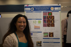
Major: Nanoscale Science and Engineering
Home Institution: SUNY Polytechnic Institute
Research Project: A Study of the Effects of Substrate Choice on Monolayer and Fewlayer NbSe2
Faculty Advisor: Prof. Jeffrey Bokor
Graduate Student Mentor: Shuang Wu
Hosting Organization: Department of Electrical Engineering and Computer Science, University of California, Berkeley
Project Abstract: Recently, transition metal dichalcogenides (TMDCs) have been investigated due to their wide range of electrical properties such as semiconductivity, superconductivity, charge density wave, etc. that are influenced by the number of layers, TMDC phase transition temperature, doping status, and choice of substrate[1]. In particular, bulk NbSe2 exhibits superconductivity at a critical temperature of 7.2K and is able to maintain its superconductive state as it approaches its two-dimensional limit despite a lowering of the critical temperature [2-3]. The primary goal of this project is to identify the number of layers and thickness of the NbSe2 on different substrates via Atomic Force Microscopy (AFM). NbSe2 was placed onto SiO2 and preliminary data regarding the transfer and characterization of these samples onto smoother target surfaces, specifically h-BN, was obtained. Further investigation is undergoing. The results of this experiment will be useful for the potential ability to realize the graphene nanoribbon-NbSe2 heterostructure as a quantum supercurrent transistor.
Undergraduate Researcher: Kevin Ye
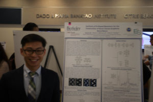
Major: Chemical Engineering and Materials Science
Home Institution:University of Southern California
Research Project: Synthesis of N-doped Monomers for the Surface Assisted-Construction of Novel Chevron Graphene Nanoribbons
Faculty Advisor: Felix Fischer
Graduate Student Mentor: Rana Mohamed
Hosting Organization: Department of Chemistry, University of California, Berkeley
Project Abstract: Graphene nanoribbons (GNRs) are quasi-one-dimensional strips of graphene which display the remarkable electronic and optical properties requisite for the next generation of innovative devices. The defect-free fabrication of long-range GNRs can be achieved through the surface-assisted polymerization of singular polycyclic aromatic precursors. Since the properties of GNRs are dependent on structural parameters such as width and edge symmetry, the electronic behavior can be precisely tuned through the design of monomeric precursors. The goal of this project is to synthesize novel nitrogen-doped precursor monomers with modified electronic properties compared to undoped graphene. In addition to modifying the band gap, the presence of the nitrogen lone pairs can create a coordinating environment for various metal centers thus leading to an entirely new class of catalytic GNRs. These novel monomers will be characterized using 1D-NMR and MALDI-TOF MS.