The E3S Research Mission
The Center for E3S was established in 2010 to employ a broad research and education approach with the goal to revolutionize two major fundamental components of digital information processing systems: the communications logic switch and the short-medium range communication of information between logic elements. These goals were pursued by four distinct research themes. Three themes focused on logic switching (Nanoelectronics, Nanomechanics, and Nanomagnetics), while an optical approach was used for communication of information (Nanophotonics). The Center for E3S addressed these grand challenges by a collaborative approach, which involved engineers, chemists, physicists, and materials scientists from five member institutions (University of California at Berkeley, Massachusetts Institute of Technology, Stanford University, University of Texas El Paso, and Florida International University).
The Fundamental Challenge

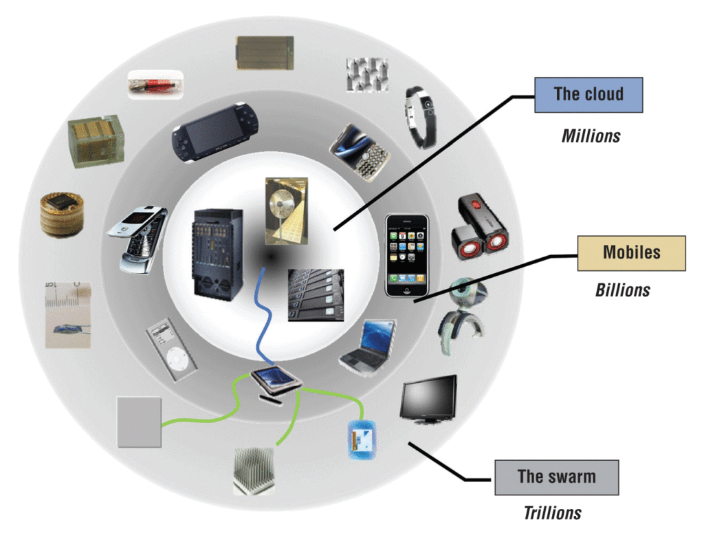
Binary bits (1’s and 0’s) are the fundamental units used to process and store information in modern electronic devices. Transistors are electrical switches that mediate the two binary states (current ON and current OFF). Integrated circuits, composed of transistors connected by wires (or “interconnects”), are the cornerstone of the modern computer. The performance of integrated circuits has improved as they become smaller. Miniaturization also has led to a decrease in power consumption. However, in the past decade, the semiconductor industry has faced severe challenges by the power density of increasingly complex integrated circuit chips. In addition, recent advancements such as cloud computing, social networking, mobile internet, wireless sensor swarms, and body-centered networks have further accelerated demand for ever increasing functionality from a fixed amount of battery energy.
The Center for E3S was formed based on the recognition that the energy used to manipulate a single bit of information was ~100,000 times greater than the theoretical limit. From its inception, the central aim of the Center employed an aggressive and disruptive approach to close this gap by seeking technological breakthroughs for two fundamental components of digital information processing systems: the communications logic switch (transistor) and the short-medium range communication of information between logic elements.
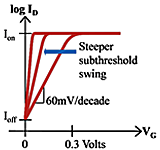
Conventional transistors suffer from a serious drawback: conduction is thermally activated. As a consequence, powering voltages of close to 1 Volt are required to provide a good ON/OFF current ratio, even as transistors become smaller and smaller. The wires connecting the transistor, however, could operate with a very good signal-to-noise ratio at voltages as low as 10 milli-Volt. Since energy consumption is proportional to the square of operating voltage, the energy currently used to manipulate a single bit of information is several orders of magnitude greater than needed in an ideal system. Therefore, a more sensitive, lower-voltage switch is needed as the successor to the conventional transistor. In addition to energy for switching, an integrated circuit chip consumes energy for communications between the transistors, through the interconnects. The power consumed by interconnects in a microprocessor chip is substantial, and can reach more than 50 percent of the total consumed power.
Research Goals and Objectives
 The research goals of the Center for E3S were set from fundamental considerations on the minimum energy needed per digital function. Part of the goal was to explore the lowest limits of each experimental approach compared to the fundamental limits, and to elucidate the factors that determine the minimum energy that each approach can reach.
E3S identified the following critical specifications for a new switch:
- Sensitivity: ~1 milli-Volt/decade, allowing switches with a swing of only few milli-Volts.
- ON/OFF current ratio: 10,000-1,000,000:1
- Current or conductance density (for miniaturization): 1 milli-Siemens/micrometer; i.e. a 1-micrometer device should conduct at ~1 kilo-Ohm in the ON-state.
These goals and objectives were pursued in four distinct, but interrelated research themes: Nanoelectronics (solid-state millivolt switching), nanomechanics (zero-leakage switching), nanophotonics (few-photon optical communication), and nanomagnetics (low-energy fast magnetic switching). Overarching these four research themes was systems integration, which checked that the component research outcomes and new scientific device concepts of the Center will actually lead to new energy-efficient system architectures, enabling future ultra-low power information technologies.
Major Accomplishments
While the research and education mission of the Center for E3S sunset in 2022, the numerous discoveries and breakthroughs achieved by E3S researchers will continue to have tremendous scientific influence on the future of energy efficient electronics.
- The Nanoelectronics Theme found that low-power tunnel-field effect transistors will be much more challenging to create, than expected. Nonetheless, researchers at E3S laid out the requirements that will guide future research, including atomic scale perfection and non-Lorentzian spectral lineshape, with graphene nanoribbons as the materials base.
- The Nanomechanics Theme demonstrated the importance of molecular functionalization on the surfaces of micro/nano-electromechanical switches that will likely become standard in the field of nanomechanics. Moreover, a groundbreaking method to directly integrate mechanical relays with standard CMOS fabrication was developed using the back-end-of-line (BEOL) interconnect (metal) layers.
- The Nanophotonics Theme discovered the antenna-LED as the missing link of optoelectronic sources for on-chip optical communication. The antenna-LED operates at low power, but at a speed comparable or faster than lasers, and allows for full on-chip integrated with other optical components.
- The Nanomagnetics Theme pointed the correct path for high-speed magnetic switching based on a new exchange-mediated mechanism. This non-classical approach enables charge-induced ultrafast switching at ~100 times higher speeds than conventional methods, bringing magnetic switching down into the picosecond range.

