Theme 1: Nanoelectronics
Faculty
Eli Yablonovitch (theme leader), Berkeley
Jesus del Alamo, MIT
Felix Fischer, Berkeley
Ali Javey, Berkeley
Jing Kong, MIT
Steven Louie, Berkeley
Vladimir Stojanović, Berkeley
The goal of the nanoelectronics research team was to develop highly energy-efficient solid-state electronic switches operating in the milli-Volt range as a replacement of the conventional transistor. A device switching at voltages two orders of magnitude lower than required in current transistors would consume 10,000-times less power—the difference of charging your cell phone every day, or once every 30 years, for example.
Challenges
Tunneling is an interfacial process, limited by the two-dimensional density of quantum states, which is ~10^12/(cm^2 eV). This desirable tunneling needs to compete with bandgap defect state density, which is a famous figure-of-merit in electronics science. In the most favorable materials systems currently used the interfacial defect density is ~10^10 /(cm^2 eV). Therefore, even after decades of electronic material investigations, the best interface state-density materials are far from being good enough. The Center for E3S has thus embarked on a search for new material systems with interface property, beyond what decades of research have previously accomplished.
Major Accomplishments
While E3S researchers have found that low-power tunnel-field effect transistors will be much more challenging to create, than expected, in the last decade, they have made tremendous progress on the path to millivolt switching. In addition, the Center for E3S has laid out the requirements that will guide future research, including atomic scale perfection and non-Lorentzian spectral lineshape.
- Fabrication and device characterization of the first 2D monolayer chalcogenide tunnel field-effect transistor.
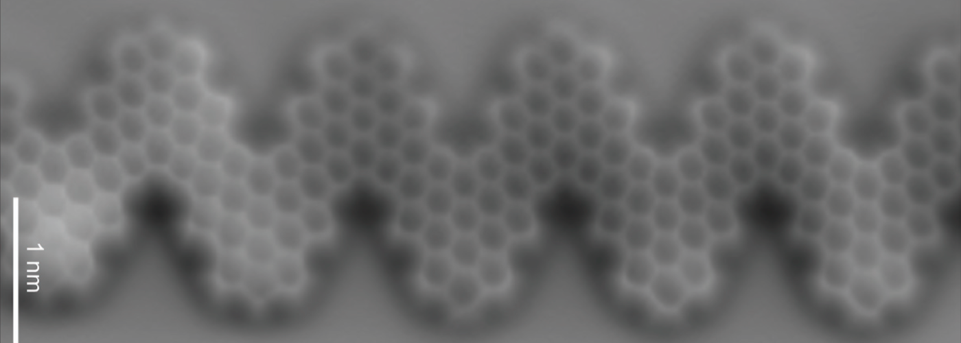
- Introduction of the field of graphene nanoribbon devices and development of a device toolbox with semiconducting, metallic, and magnetic graphene nanoribbons.
- Incorporation of graphene nanoribbons into device architectures and demonstration of functioning graphene nanoribbon field effect transistors.
- The first experimental demonstration of sub-10-nm diameter broken-gap GaSb/InAs vertical nanowire diodes and InGaAs
- Demonstration of the first bilayer dual-gated tunnel field-effect transistor, in which tunneling occurs across an undoped nanoscopic film, with gate electrodes on both sides.
- Development of chemical passivation and electrostatic doping methods to achieve extra-ordinary improvement in photoluminescence quantum efficiency close to 100 percent.
- Using semi-metal contacts, a record high performance ON current was achieved for 2D devices, approaching the performance of bulk semiconductor devices.