E3S REU Participants and Projects: 2012
Undergraduate Researcher: Franiece Bennett
 Major: Electronics Engineering
Home Institution: Norfolk State University
Research Project: Dynamic Graphical Representation of Vertical Cavity Surface Emitting Lasers
Faculty Advisor: Prof. Connie Chang-Hasnain
Graduate Student Mentor: Wai-Son (Wilson) Ko
Hosting Organization: Electrical Engineering and Computer Sciences Department, UC Berkeley
Project Abstract: The incorporation of photonics with silicon CMOS can potentially lessen energy consumption of data communication in microprocessors. The effectiveness of interfacing both electronic and optical components in a device requires testing, graphical representation with the use of Matlab, analysis, and interpretation of the measured results. The testing tProject posterin monitors the change in voltage distributed onto a device for a given pump current and the plotting of the IV curve in comparison to the correct characterization curve of the electronic component. The optical setup incorporates the monitoring, graphing, and interpretation of the light emitted from the laser components.
Project poster
Undergraduate Researcher: John Bryant
 Major: Electrical Engineering
Home Institution: Florida International University
Research Project: Low Power Nanomagnet Control
Faculty Advisor: Prof. Jeffrey Bokor
Postdoc Mentor: Dr. Mark Nowakowski
Hosting Organization: Electrical Engineering and Computer Sciences Department, UC Berkeley
Project Abstract: The field of nanomagnetics has the potential to open new pathways for energy-efficient data processing and storage. Nanomagnets rely on dipolar coupling to transfer data across a circuit with potentially 106 times more efficiency than traditional electrical buses1. One of the challenges of this technology is to reduce the energy needed to clock a series of nanomagnetics. Much of the power saved via nanomagnetic data transfer is lost by the power required to apply an external magnetic field. One solution is to create nanomagnetic composite multiferroic heterostructures composed of piezoelectric and magnetostrictive materials to manipulate local on-chip magnetic fields by modulating strain to control the magnetoelastic energy at the interface. We model the electrical field required to induce a magnetic easy axis reorientation and measure the anomalous Hall effect transport properties of terfenol-D/piezoelectric heterostructure devices to characterize the magnetoelastic interface. Project poster
Undergraduate Researcher: Anna Colleen Crouch
 Major: Polymer and Fiber Engineering
Home Institution: Georgia Institute of Technology
Research Project: Magnetotransport across Conducting Domain Walls in Bismuth Ferrite
Faculty Advisor: Prof. Ramamoorthy Ramesh
Postdoc Mentors: Dr. Guneeta Singh Bhalla & Dr. John Heron
Hosting Organization: Materials Science & Engineering Department, UC Berkeley
Project Abstract: Over the past few decades, complex perovskites oxides have been extensively studied due to the wide range of functional electronic phases they exhibit including highly correlated electron behavior, superconductivity, ferroelectricity and magnetism. Multiferroics are a group of oxide perovskites which possess both a ferroelectric polarization and a magnetic order which are coupled. Bismuth ferrite is a prototypical multiferroic with an additional unique characteristic. While the bulk material is insulating, the ferroelectric domain walls separating two regions of differently oriented electric dipoles conduct electricity. In this work, we probe the conducting domain walls via magnetotransport measurements in order to better understand their electronic and magnetic properties. Due to the domain wall’s size and control achieved thus far in spatial control, we explore their potential for electronic device applications. Project poster
Undergraduate Researcher: Daniel Drew
 Major: Materials Science & Engineering
Home Institution: Virginia Polytechnic Institute and State University
Faculty Advisor: Prof.Jeffrey H. Lang and Vladimir Bulovic
Mentors: Farnaz Niroui & Dr. Annie Wang
Hosting Organization: Electrical Engineering and Computer Sciences Department, MIT
Undergraduate Researcher: Chen Dan Dong
 Major: Applied Math and Electrical Engineering
Home Institution: Massachusetts Institute of Technology
Research Project: Study of Fully Depleted SOI MOSFET Performance for Power-Efficient Analog Circuit Applications
Faculty Advisor: Prof. Tsu-Jae King Liu
Postdoc Mentor: Dr. Nuo Xu
Hosting Organization: Electrical Engineering and Computer Sciences Department, UC Berkeley
Project Abstract: The impact of back biasing on tuning analog circuit performances for Fully Depleted SOI (FD-SOI) MOSFET is studied. Several analog performance metrics, including transconductance (Gm), Gm/Id ratio, linearity and low-frequency noise are evaluated for nanometer-gate-length devices, which provide insights for power-efficient circuit design based-on FD-SOI technology platform. Project poster
Undergraduate Researcher: Steven Drapcho
 Major: Physics
Home Institution: Massachusetts Institute of Technology
Research Project: Strain Tuning of Structural and Electronic Properties of (Ba0.8Sr0.2)TiO3
Faculty Advisor: Prof. Sayeef Salahuddin
Graduate Student Mentor: Asif Khan
Hosting Organization: Electrical Engineering and Computer Sciences Department, UC Berkeley
Project Abstract: The study presents evidence of control over the structural and electrical properties of ferroelectric thin films of epitaxial (Ba0.8Sr0.2)TiO3 (BSTO) through strain tuning. We use pulsed-laser deposition (PLD) to grow thin films of SrRuO3-buffered BSTO on four different substrates: DyScO3 (DSO), GdScO3 (GSO), SrTiO3 (STO),
and NdScO3 (NSO). Using x-ray diffraction techniques, we find that the BSTO out-of-plane c lattice parameter decreases with increasing tensile strain as expected. We discover that the dielectric constant of BSTO decreases with c/a and tProject posterfore increases with tensile strain due to increased dielectric polarizability. Frequency and Rayleigh analysis of the dielectric constant show high crystal quality free from defects, indicating that the effect of strain on the dielectric constant is due to intrinsic rather than extrinsic effects. Project poster
Undergraduate Researcher: Robert Orleans-Pobee
 Major: Electrical Engineering and Physics
Home Institution: Virginia Tech
Research Project: Investigating Band-Edge Sharpness in GaSb/InAs Heterojunctions for Use in TFETs
Faculty Advisor: Prof. Eli Yablonovitch
Graduate Student Mentor: Jared Carter
Hosting Organization: Electrical Engineering and Computer Sciences Department, UC Berkeley
Project Abstract: While miniaturization has continued to develop according to Moore’s law, yielding increased electronics performance, the overall pace of improvement is beginning to slow because power requirements have remained largely the same. The leading source of power consumption in modern circuits is the Metal-Oxide Field-Effect Transistor (MOSFET); tProject posterfore, in order to reduce power consumption and continue the trend of increased performance, a mechanism needs to be found to operate these transistors at lower voltages. One proposed low-voltage alternative to the MOSFET is the Tunneling Field-Effect Transistor (TFET), which operates by manipulating the quantum tunneling effect in a P-N junction. For tunneling in a junction, the conduction band on one side must line up with the valence band on the other, a condition that is met in GaSb/InAs heterojunctions. However, in order for these heterojunctions to be viable in transistors, the band edges must be extremely sharp. We intend to investigate the sharpness of these band edges, using a variety of techniques, most notably developing a circuit for use in band-edge spectroscopy.
Project poster
Undergraduate Researcher: Benjamin Osoba
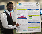 Major: Electronics Engineering
Home Institution: Norfolk State University
Research Project: Simulation of 2D InAs/GaSb Heterojunction TFET
Faculty Advisor: Prof. Chenming Hu
Postdoc Mentor: Dr. Yuping Zeng
Hosting Organization: Electrical Engineering and Computer Sciences Department, UC Berkeley
Project Abstract: In this project, the possibilities for 2D simulation using the Nextnano3 simulation program were explored. Specifically, a previously operational 1D simulation script was altered and developed into that of a 2D simulation. The 2D script provides a template for the group to use, allowing the 2D simulation to become more accessible and understandable. In this instance, the program was used to analyze the characteristics of a 2D heterojunction InAs/GaSb TFET. The 2D simulation proved operational, without errors in script which would result in incomplete compilation. TProject poster are still some components of the program which need further analysis, such as the color-coded outputs which do not yet display a color-key.
Project poster
Undergraduate Researcher: Ken Wilson
 Major: Biochemistry and Mathematics
Home Institution: Bloomfield College
Faculty Advisor: Prof. Timothy M. Swager
Graduate Student Mentor: Ahmed Eilaf
Hosting Organization: Department of Chemistry, MIT
Undergraduate Researcher: Peida Zhao
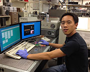 Major: Electrical Engineering
Home Institution: UC San Diego
Research Project: Investigating Material Properties of Tantalum Selenide and Tantalum Sulfide and Their Compatibilities in
Low Energy Devices
Faculty Advisor: Prof. Ali Javey
Graduate Student Mentor: Hui Fang
Hosting Organization: Electrical Engineering and Computer Sciences Department, UC Berkeley
Project Abstract: We fabricated back-gate and top-gate FET devices using two different transition metal dichalcogenides (TMDC) systems, specifically TaS2 and TaSe2, as the channel material of a FET-like device. Previous studies of the TMDC family have indicated semiconducting behavior of TaSe2 and TaS2 (with a bandgap of 0.25eV and 0.1eV respectively) at low temperature owning to the formation of a gap in the Fermi surface, associated with the charge density wave effect (CDW). Our studies however, have shown metallic behavior of both systems in bulk dimension (at ~6-7nm) at room temperature and low temperature with no gate dependence. Further investigations of the material as we thin down layer thickness (<5 nm thick or <7 monolayers) have shown a “metal to insulator” transition wProject poster the materials cease to conduct. Our investigation of the fundamental TaS2 and TaSe2 characteristics will hopefully pave the way for a newer generation of monolayer FETs using TDMC materials other than MoS2 and WSe2.
Project poster
